Prologue
It was a great Friday, the 31st of August 2007 at 22:25:25 I etched my first PCB ever at home, it was the second year of high school and I was so excited about it. After doing some research and information gathering from some friends who happen to be great engineers.
This is how I got started with electronics — believe it or not, by building my first PCB using Ferric Chloride FeCl3 solution with 60% concentration and a blank copper Printed Circuit Board (PCB). Eventually, this partially paved the way to me learning to write computer programs as well.
I thought I would start my first post in this weblog with a brief history of me 😄
Theory
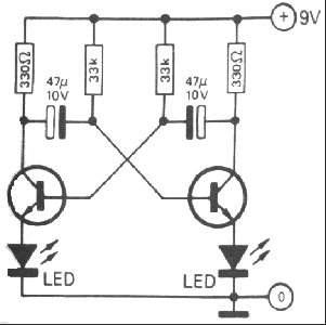
Using two transistors setup as an Astable multivibrator circuit. Principally, the two capacitors switch their states from being charged to drained, which in turn triggers the transistors. The transistors control each LED state which causes it
There is a nice visualization on this website using a Java Applet for the astable multivibrator.
The first schematic diagram which I received from an online friend who is an Electronics Engineer and was a PhD candidate in Canada at that time, we used to discuss electronics from time to time:
Bill of Materials (BOM) ☺️
| Quantity | Item | Value |
|---|---|---|
| 2 | LED | Green / Red |
| 2 | NPN Transistor | BC547 |
| 2 | Capacitor | 47 µF |
| 2 | Resistor | 33 kΩ |
| 2 | Resistor | 330 Ω |
| 1 | Connector | 9V Snap |
| 1 | Battery | 9V |
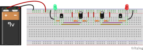
Modern breadboard version (using Fritzing)
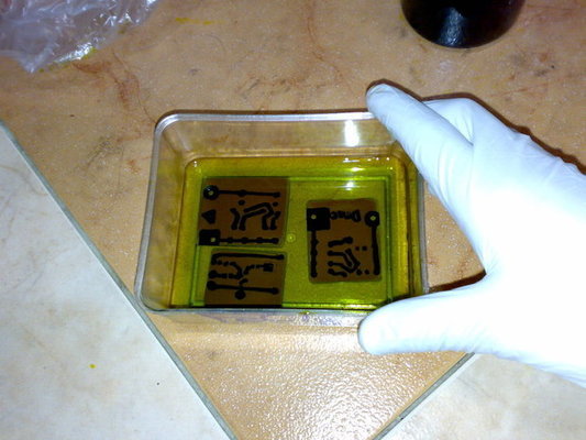
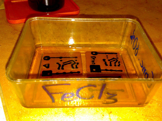
PCB etching at home using FeCl3
I etched this PCB after drawing the traces using a permanent ink marker on the copper layer.
Photos from 2007 — You might notice the double layers of gloves; well yeah, I was a bit worried since it was the first time I handle FeCl3 😉 :
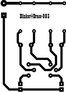
Proper PCB layout?
Later, I did a better PCB layout in Proteus, however, I no longer use it, since I started using either KiCad or Eagle nowadays — basically since I switched to Linux in 2009.
